

原文链接:https://doi.org/10.1039/D3NR04615J
Wafer-scale Patterning of High-resolution Quantum Dot Films with a Thickness over 10 µm for Improved Color Conversion
Shenghan Zou, Yuzhi Li and Zheng Gong
Abstract
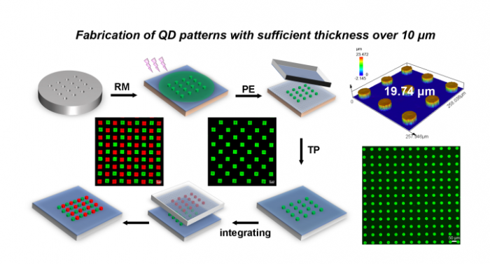
Quantum dots (QDs) are promising color conversion materials for efficient full-color micro-LED display owing to their high color purity and wide color gamut. However, achieving high resolution QD patterns with enough thickness for efficient color conversion is challenging. Here, we demonstrate a facile and compatible approach by combining replicate molding, plasma etching and transfer printing to produce QD patterns with sufficient thickness over ten micrometers in a wide range of resolutions. Our technique can remarkably simplify the preparation of QD inks and minimize optical damages to QD materials. The pixel resolution and thickness of QD patterns are controllable by well defining the microstructures of molding template and the etching process. The transfer printing process allows QD patterns to be assembled sequentially onto a receiving substrate, which will further improve the original pixel resolution and avoid repetitive optical damages to QDs during the patterning process. Consequently, various QD patterns can be fabricated in this work, including perovskite quantum dot (PQD) patterns with a pixel resolution up to 1270 ppi and maximum thickness up to 19.74 μm, a wafer-scale high resolution PQD pattern with sufficient thickness on a flexible substrate, and a dual-color pattern comprised of green PQDs and red CdSe QDs. Furthermore, those fabricated QD films with thickness over 10 μm show improved color conversion when integrated onto a blue micro-LED, revealing the potential of our technique for full-color micro-LED displays.