分享到
实验室简介
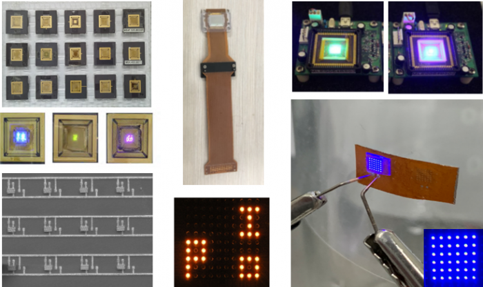
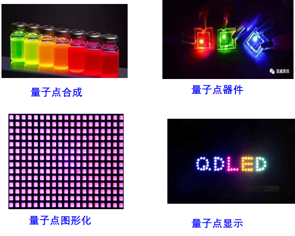
欢迎访问新型显示技术实验室!新型显示技术实验室成立于2017年4月,由广东省科学院半导体研究所学科带头人龚政教授创立。该实验室主要从事新型显示材料、器件及应用方面的研究。面向显示领域巨大的市场需求和产业化需求,研发基于Micro-LED、量子点等材料和器件的新一代显示技术,以满足高分辨率、低功耗、长寿命、响应速度快的一些应用场景:如可穿戴电子消费品、智能眼镜、智能手表、虚拟现实头盔、高清电视等。
本实验室诚邀海内外各级人才加盟,包括资深研究员/副研究员/青年研究员/助理研究员等岗位若干。
欢迎与我联系,招聘具体信息参见:职位招聘
代表性论文
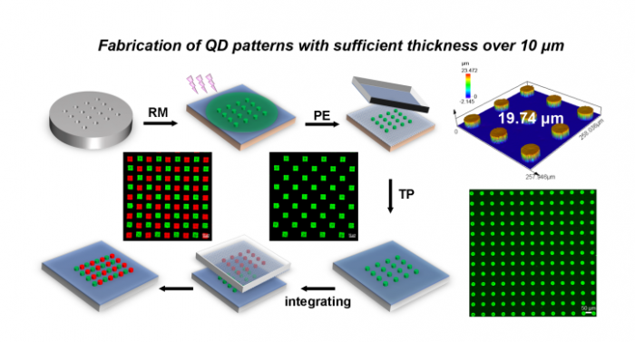
- “Wafer-scale Patterning of High-resolution Quantum Dot Films with a Thickness over 10 µm for Improved Color Conversion“,Nanoscale, 2023,15, 18317-18327, https://doi.org/10.1039/D3NR04615J
- "Insight into the evolution of electrical properties for Schottky-barrier IGZO thin-film transistors with Cu-based Schottky contacts", Appl. Phys. Lett. 123, 103503 (2023) https://doi.org/10.1063/5.0159184
- “Noble‐Metal‐Free,Polarity‐Switchable IGZO Schottky Barrier Diodes”,IEEE Transactions on Electron Devices,2023, doi:10.1109/TED.2023.3267755
- “High-Performance Sputter-Prepared Metal-Oxide Thin-Film Transistors Based on Solution-Processed Targets”, IEEE Electron Device Letters, 2023. Doi: 10.1109/LED.2022.3224920. https://ieeexplore.ieee.org/document/9964213
- “Laser-based Micro/Nano-Processing Techniques for Microscale LEDs and Full-color Displays”, Advanced Materials Technologies, 2022, 2200949. https://onlinelibrary.wiley.com/doi/full/10.1002/admt.202200949
- "Transfer Printed, Vertical GaN-on-Silicon Micro-LED Arrays With Individually Addressable Cathodes", IEEE Transactions on Electron Devices, 2022, Doi:10.1109/TED.2022.3202152. https://ieeexplore.ieee.org/document/9882009.
- "Fabrication of Schottky Barrier Oxide Semiconductor Thin Film Transistors Via a Simple AluminiumReaction Method", IEEE Electron Device Letters, 2022 ,Doi: 10.1109/LED.2022.3204937. https://ieeexplore.ieee.org/document/9881597
- “Large-scale programmable assembly of Micro-components for advanced electronics via light-regulated adhesion and polymer growth”,npj Flexible Electronics 6, 44 (2022)
- “High-Performance Inorganically Connected CuInSe2 Nanocrystal Thin-Film Transistors and Integrated Circuits Based on the Solution Process of Colloidal Synthesis, Ligand Exchange, and Surface Treatment”,Chemistry of Materials,33, 8775−8785(2021)
- “Effective defect passivation of CsPbBr3 quantum dots using gallium cations toward the fabrication of bright perovskite LEDs”,Journal of Materials Chemistry C, 9(34), 11324–11330(2021).
- [Invited Review] Layer-Scale and Chip-Scale Transfer Techniques for Functional Devices and Systems: A Review,Nanomaterials 11 (4), 842 (2021)
- Wafer-Scale Micro-LEDs Transferred onto an Adhesive Film for Planar and Flexible Displays, Advanced Materials Technologies, 2000549(2020).
- 【Invited】: Applications and challenges of Micro-pixelated light-emitting diode arrays,SID Symposium Digest of Technical Papers ,2018
- "Direct LED writing of submicron resist patterns: Towards the fabrication of individually-addressable InGaN submicron stripe-shaped LED arrays",Nano Research 7 (12), 1849-1860(2014)
- "Micro-LED pumped polymer laser: A discussion of future pump sources for organic lasers", Lasers & Photonics Review. 7, No. 6, 1065–1078 (2013)
- "CMOS-controlled color-tunable smart display", IEEE Photonics Journal 4,1639(2012)
- "Size-dependent efficiency and efficiency droop of blue InGaN micro-light emitting diodes", Applied Physics Letters 101 (23), 231110(2012)
- "Hybrid organic/GaN photonic crystal light-emitting diode", Applied Physics Letters 101 (14), 141122, 2012
- Size-dependent light output, spectral shift, and self-heating of 400 nm InGaN light-emitting diodes", Journal of Applied Physics 107 (2010) 013103
- Matrix-addressable micropixellated InGaN light-emitting diodes with uniform emission and increased light output", IEEE Transactions on Electron Devices 54 (2007) 2650-2658.
- "A Vertically Integrated CMOS Microsystem for Time-Resolved Fluorescence Analysis", IEEE Transactions on Biomedical Circuits and Systems 4 (2010) 437-444.
- "High-Speed Visible Light Communications Using Individual Pixels in a Micro Light-Emitting Diode Array", IEEE Photonics Technology Letters 22 (2010) 1346-1348.
- "Microstripe-array InGaN light-emitting diodes with individually addressable elements", IEEE Photonics Technology Letters 18 (2006) 1681-1683.
- "Formation of GaAs/AlGaAs and InGaAs/GaAs nanorings by droplet molecular-beam epitaxy", Applied Physics Letters 87 (2005)093116.
- "Surface morphology control of strained InAs/GaAs(331)A films: From nanowires to island-pit pairs", Applied Physics Letters 86 (2005)013104.
- "Complex quantum ring structures formed by droplet epitaxy", Applied Physics Letters 89 (2006)031921.
访问量:1245


